Syncopated Systems™
Seriously Sound Science™
|
Syncopated Systems™
Seriously Sound Science™
|
| Home | About | Library | Contact |
An Introduction to Printed Circuit BoardsSyncopated Systems regularly designs and develops products incorporating electronic circuits. In doing so, one of its most fundamental tasks is the physical implementation of those circuits through the design of printed circuit boards and the outsourcing of their fabrication and assembly. Each time it performs these tasks, as summarized in this article, Syncopated demonstrates expertise in the disciplines of computer science, electrical engineering, mechanical engineering, component engineering, purchasing and project management. Printed circuit boards create electrical connections between electronic components – and sometimes components themselves – in the most cost-effective manner for many applications including general-purpose computers and consumer products. By recognizing and understanding applicable rules of physics and available manufacturing processes and costs, skilled printed circuit designers may create circuits that behave as desired at minimal total cost to produce. This article surveys common types of printed circuit boards and the history of their development, as well as basic design processes, considerations and tools needed to create them. Table of Contents
Printed Circuit Board DefinedA printed circuit board, commonly abbreviated p.c.b., consists of at least one rigid planar electrically-insular substrate laminated with at least one electrically-conductive layer (usually metal foil), which is printed with a pattern designed to make specific desired connections between the pins of components mounted or otherwise attached to it. Other Printed CircuitsDerived from p.c.b. fabrication processes are those used to create flexible printed circuits and semiconductor integrated circuits (commonly called silicon "microchips" or "chips"). Though detailed description of these circuits falls outside the scope of this article, they are summarized below. Flexible Printed CircuitsFlexible printed circuits, as the name implies, are similar to printed circuit boards in having one or more conductive metal layers printed on an insular substrate, but the substrate used is a thin sheet of a flexible plastic such Mylar (a brand of biaxially-oriented polyethylene terephthalate, or boPET) polyester film. Because the substrate plastics used often have melting points well below that of the solder used to connect components to rigid printed circuit boards, connections to flexible printed circuits are usually made via crimped contacts and/or friction-locked connectors. Flexible printed circuits are often used in electromechanical devices such as keyboards, disc drives and liquid-crystal displays. Integrated CircuitsIntegrated circuits (abbreviated i.c.s) are fabricated on a much smaller scale using similar printing techniques. Though they are created using processes very similiar to and ulitmately derived from p.c.b. processes, detailed description of flexible printed circuits and integrated circuits falls outside the scope of this article. NomenclatureDespite the industry's history of more than 100 years of electrical engineering and 50 years of printed circuits, there is still little accepted commonality in the names used to describe printed circuits. Some refer to a printed circuit board as a printed wiring board, abbreviated p.w.b.; it is a naive term, implying failure to recognize the electrical properties of the board's substrate and patterns printed thereupon. As the density of printed circuit board integration increases, the values of these properties become much less negligible, so the term p.w.b. should be deprecated. Some organizations, allegedly including I.B.M., insist upon using the word "card" in place of "board", apparently to help differentiate electrical circuits from lumber. Both words adequately describe the planarity of the substrate, so both are acceptable and may be used interchangeably. However, the word "board" is more commonly used and therefore more commonly understood, so its usage should be preferred. Mating RelationshipsPrinted circuit boards that are rigidly mounted together through only connectors (without wire or cable between them) are often described in terms of their mating relationships.
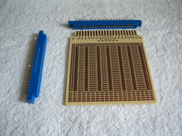
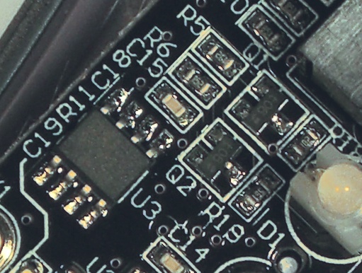
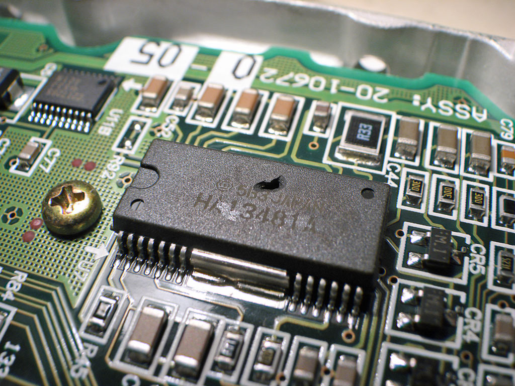
LayersA printed circuit board is constructed through the combination of several planar layers that are themselves formed through additive and subtractive processes. The simplest printed circuit boards are formed by placing a conductive layer on an insulator and removing (via chemical or mechanical means) the conductive material from areas in which it is not desired. InsulatorsA printed circuit board substrate is an electrical insulator that provides the p.c.b. its rigid planar structure. The materials used for p.c.b. substrates and their flame-retardance ("f.r.") ratings vary, from FR-0 pressed cellulose (paper) to ceramic tile, but FR-4 epoxy fiberglass is most commonly used in the United States. ConductorsEach metal layer consists of metal foil (such as copper, Cu) laminated to the substrate which is printed using a photographic process (described in more detail below) with a resistive mask, etched with acid (such as ferric chloride, FeCl3), then the mask and any residual acid are washed off. Connections between multiple metal layers were first made through pins soldered on top and bottom and later through plated-through holes; a connection between metal layers without using the pins of a component are made via a hole called a via (pluralized "vias"). Solder MasksSolder masks are usually green, though they may be any color. Solder masks assist averting solder bridges (which cause undesired short circuits) in the assembly process by block the flow of liquified solder when components are populated onto the printed circuit board. Most modern printed circuit boards include top and bottom solder mask layers, which have been historically silkscreen-printed but are now more commonly printed using liquid photo-imageable (l.p.i.) processes. Component LegendsLegend layers, as with solder masks, have been historically silkscreen-printed but are now more commonly printed using l.p.i. processes; they are still often (and usually incorrectly) referred to as "silkscreen" or just "silk" layers. Legend layers are usually the outermost layers printed over the solder mask, if present. Often white, though they may be any color (usually contrasting that of the solder mask and/or substrate onto which it is printed), they identify the intended location and orientation of components to be mounted to the board, and often include other information that may be of service to those assembling, troubleshooting or using the assembly built on the board. Other Design LayersIn addition to the patterns used to print each layer, each printed circuit board design usually also includes a mechanical drawing used to specify how the p.c.b. is to be fabricated; this fabrication drawing is often refered to as the fab. drawing. For most modern printed circuit boards, especially those having more than two copper layers, this drawing also includes a cutaway side view illustration, often referred to as a layer stack up. Though technically not parts of the printed circuit boards themselves, the designs of most modern printed circuit boards also include the pattern for one or two solder paste stencils. Solder paste stencils are thin metal sheets with many small holes used as a mask in the application (with a squeegee) of solder paste prior to the placement of surface-mounted components on the p.c.b. during the assembly process. Most openings in each solder paste stencil are usually of roughly the same shape of and coincident to, but slightly smaller than, each exposed metal pad on the p.c.b. to which a component lead is to be connected; these shapes are said to share a common centroid. Because of the similarities in the patterns of stencils and the corresponding solder masks on the p.c.b., stencil designs may sometimes be derived from solder mask layers. Design PhysicsThe function of electronic circuits is governed by relatively simple concepts in chemical and electromagnetic physics. Among them, conduction and induction apply most fundamentally to the design of printed circuit boards. ConductionConduction refers to the flow of electrons through a conductor. For historical reasons, conductivity is expressed as the multiplicative inverse of resistance. The resistance of a planar conductor – such as a metal layer of a printed circuit board – is expressed in terms of its sheet resistance, which is measured in Ohms per square area of the conductor. Printed circuit board designers create desired conduction paths and avoid creating undesired conduction paths for all signal and power nets. InductionInduction refers to the capacitive coupling of electrical potential between nearby electrodes, which include any material that is capable of conducting electrons, such as metals or semiconductors; on printed circuit boards, all metal areas (including hole plating) are electrodes. Induction may be used for desired effects – such as creating capacitance for power supply decoupling between adjacent layers – or may cause undesired effects – such as increased noise between signal nets, commonly referred to as crosstalk. The degree of induction increases as a square function as proximity between electrodes increases. Fabrication and Assembly Process HistoryThe first U.S. patent for a printed circuit board (Patent 2,756,485) – was issued in July 1956 (for the application filed 1950/08/28) to Moe Abramson and Stanislaus F. Danko (both of New Jersey) and assigned to the United States of America via the the secretary of the U.S. Army. Single-Sided Etched CopperThe earliest printed circuit boards were those with a single-layer of bare copper laminated to a subtrate. A desired pattern could then be created in the copper using a photographic, photochemical process. As summarized above, this process generally involved:
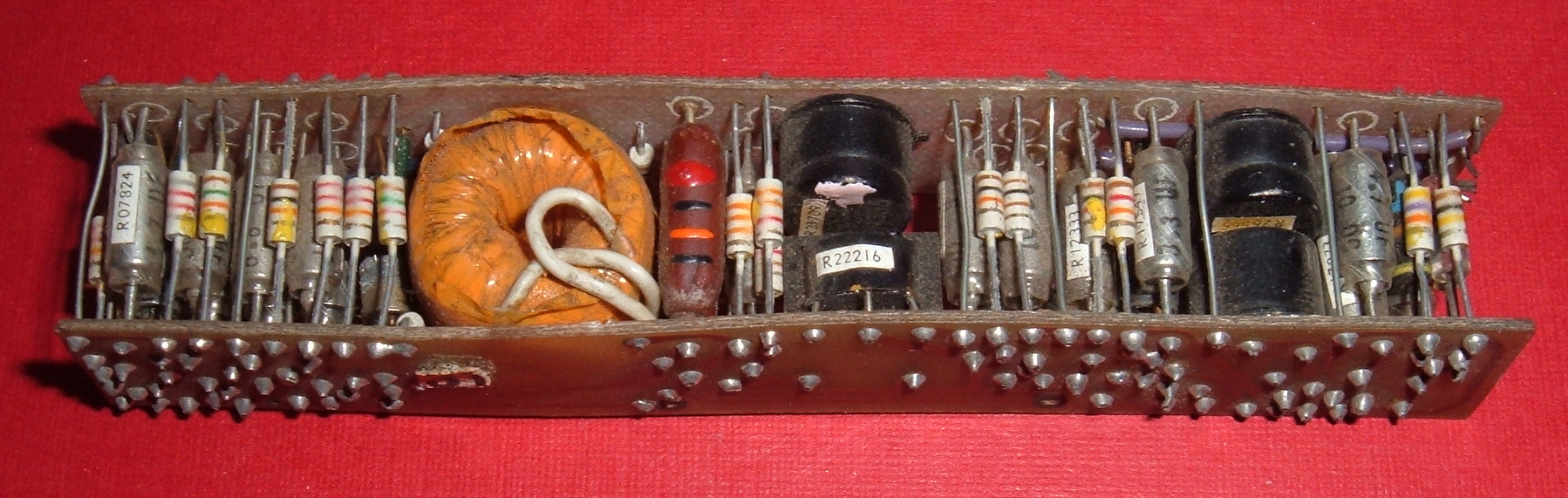
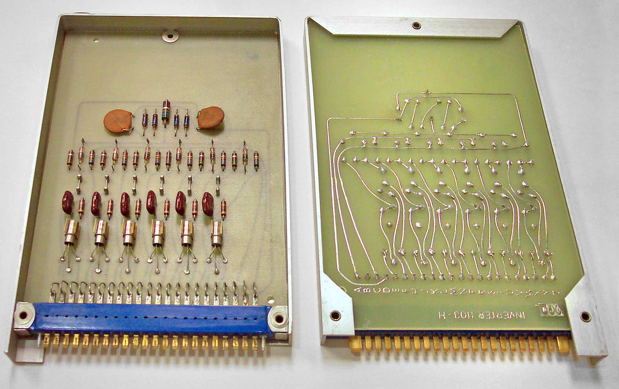
Cordwood Circuit Assembly MethodThe first two of the orignial patent's six claims essentially refer to a method of "plural deck framing" that has become known as the "cordwood" circuit construction method, which is no longer in common practice. Using this method, axially-leaded components are stacked together like cordwood.
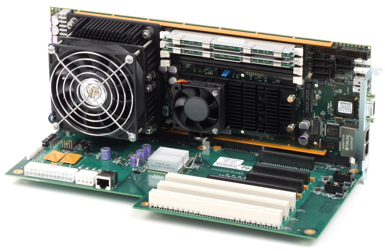
Proliferation of Solder MasksBy 1980, solder masks on top and bottom (typically using the same pattern) and a separate legend printed on the component side were commonly added to printed circuit boards. The wave soldering process used during the circuit assembly process allowed solder to wick under the solder-side solder masks; sometimes these amounts were large enough to erode away parts of the solder mask. Around this time, some printed circuit boards were fabricated with edge connectors, which extended to the edge on the p.c.b. wide fingers of copper electroplated with gold (Au) finish over a nickel (Ni) barrier layer. This type of p.c.b. was used, for example, in the Apple II and Atari 800 home computers released in 1977 and 1982, respectively. With the 1981 release and subsequent proliferation of the I.B.M. PC, the availability of p.c.b. computer-aided design (cad) software also spread. Surface-Mounted TechnologyIn the 1980s, surface-mounted technology (s.m.t.) had emerged as a new method for packaging components and assembling circuits.
Proliferation of LaminationInto the new millenium, the costs associated with the lamination and alignment of more than two metal layers had decreased to the point that fabricating printed circuit boards with internal metal layers was no longer significantly more expensive than producing those without. However, due to many market factors (including monopolization), the costs of software tools needed to design printed circuit boards with internal metal layers still remains prohibitive for many designers. Reduction of Hazardous SubstancesUse of lead (Pb) in printed circuit boards and other electronic components – other than in lead-acid batteries (in which lead may be easily identified, contained and recovered) – is being phased out, largely due to the European Union's Directive on the Restriction of the Use of Certain Hazardous Substances in Electrical and Electronic Equipment (2002/95/EC, commonly referred to as "reduction of hazardous substances", r.o.h.s. or "RoHS"), which is described in more detail below. Design ProcessCreating a printed circuit board is a process that typically includes many parties. Their responsibilities are fundamentally defined in terms of what each party delivers to another. PartiesThe parties involved in creating a printed circuit board assembly typically include – in approximately this order – the circuit's:
The electrical designer is the layout designer's client, but the relationships between the other parties generally take either one of two forms. Typically, the layout designer acts as an agent of its client; in this case it is the layout designer's client who issues a purchase order to the fabricator. Less commonly, the layout designer adds value by becoming the client of the fabricator (and sometimes the assembler) and sells finished products to the designer's client. Fabricators increasingly add value by providing photographic mask and solder paste stencil creation services (even if outsourced). Component engineers facilitate design documentation and communication between design engineers and purchasing agents to assure the continued supply of components needed for manufacturing by identifying, verifying, and documenting the potential interchangeability of different components offered by different manufacturers. Assemblers increasingly add value by providing component purchasing services. Those that do are referred to as "turnkey" assemblers or manufacturers; those that do not are referred to as "consignment" assemblers or manufacturers, for the components consigned to them by their clients. Design ToolsCreating a printed circuit board generally requires two computer-aided design (cad) software products: one to "capture" (through digitization) its schematic diagram(s) and one to "lay out" its physical design; data files containing the part list and net list are created using the former and used by the latter. In addition, perhaps the most valuable printed circuit board design tool available today – especially for lone designers or those within small organizations – is the extensive Web-based Digi-Key electronic component catalog. This enables some electrical and layout engineers to perform many basic functions usually performed by component engineers within larger organizations, such as identifying components to use in a design, though often with many limitations and/or errors. Third-Party Layout ToolsPrinted circuit board design software was first created for mainframe computers, but soon spread with the proliferation of personal computers. The early widespread availability of good software tools costing only $500-1000 allowed many to design printed circuit boards. However, today most of the software tools have been monopolized by only a few vendors, artificially increasing p.c.b. development costs through deadweight loss. (wiki:Monopoly) The dominant p.c.b. cad software vendors and products today include:
Fabricator-Supplied Layout ToolsFortunately for designers of relatively simple printed circuit boards, competitive pressure between p.c.b. fabricators has spawned them to introduce simple schematic capture and p.c.b. layout cad software products. These are made available to designers free of charge, but only allow the design to be fabricated by the supplier of the software product. For some designs and designers, the costs saved in cad software may offer a good trade for the limitations of the crude software tools, which include non-portability of the work invested in each design and lack of automated design rule checks. Fabricators (likely fabricator syndicates) supplying p.c.b. cad software include: Note that both of the above fabricate two- and four-layer printed circuit boards with several options. However, the last time I evaluated the software offered by each, I qualified only ExpressPCB, but only for two-layer p.c.b. designs. As I recall, the cad software products I evaluated did not adequately display or allow the designer to edit data for interior layers to be sufficiently useful to create four-layer printed circuit boards. (For more information about the process of qualifying vendors, see the article Operations Management.) DeliverablesAfter a circuit's electrical design is complete, the design of its p.c.b.(s) may begin. Circuit DesignAt that point, the circuit designer typically delivers to the layout designer:
After the p.c.b. design is complete, the circuit's electrical designer is responsible for checking and accepting the final layout before sending the design to fabrication. Because layout designers often work very closely with p.c.b. fabricators (sometimes tailoring the design and design rule check to a particular fabricator's capabilities), a layout designer will often release the design's deliverables directly to the fabricator. Layout DesignDeliverables from the layout designer typically include:
Ultimately, all of the deliverables from the layout designer usually (per contract) become the property of the layout designer's client and are considered "work for hire". FabricationFabricators deliver the printed circuit boards themselves, but increasingly also sell solder paste stencils used by assemblers. By convention, non-populated printed circuit boards from the first fabrication lot are usually allocated and kept for reference by the circuit's electrical designer, layout designer and assembler. IndustryRegulatory AgenciesWithin the United States, the printed circuits industry per se is the subject of relatively little direct regulation. However, the manufacture, use and sale of its products are often regulated. Manufacturing of electronic circuits is usually governed by the U.S. Congress's Environmental Protection Agency (E.P.A.) and similar state bodies. In addition, the electronics industry has widely accepted movement toward and acceptance of the European Union's Directive on the Restriction of the Use of Certain Hazardous Substances in Electrical and Electronic Equipment (2002/95/EC, commonly referred to as "reduction of hazardous substances", r.o.h.s. or "RoHS"), which restricts the use of lead (Pb), mercury (Hg), cadmium (Cd), hexavalent chromium (Cr6+ or "chromium xxx"), polybrominated biphenyls (p.b.b.) and polybrominated diphenyl ether (p.b.d.e.). (wiki:RoHS) This trend has also introduced the practice of informing consumers of the presence of hazardous substances in products, such as mercury used in the backlights of flat-panel displays. Generally, the sale and use of electronic products are governed by the U.S. Congress's Federal Communications Commission (F.C.C.), usually though its Part 15 and Part 68 rules regarding radiated and conducted electromagnetic emissions, respectively. Circuits that use or produce dangerously high voltages are often required by many governmental agencies to gain approval from the domestic insurance industry's Underwriters Laboratories (U.L.). By convention, "high voltage" circuits are those in which the potential energy present between any two points may be at least 42.5 volts, though regulatory limits and industry convensions often vary from 40 to 45 volts. Some electronic products are subject to further restrictions, depending on the technologies they employ. The federal government may restrict the exportation of certain products (including computer software) that it deems may potentially be used to create weapons of war (as munitions), and these must bear export restriction notices. Devices that use radiation not within the electromagnetic spectrum, such as X-ray equipment and atomic reactors, are usually restricted by the Department of Energy. Trade AssociationsThe dominant trade organization for the printed circuits industry is I.P.C.. Founded in 1957 as the Institute for Printed Circuits, it broadened its scope in the 1990s to include more electronics assembly companies, changing its name to the Institute for Interconnecting and Packaging Electronic Circuits; after realizing that few people in the industry could remember the full name and meaning, it changed its name again in 1999 to just I.P.C.. Other major trade organizations closely associated with the design and fabrication of printed circuit boards include:
Related ReadingFor more general information about electrical engineering, see An Introduction to Electrical Systems. For more information about the process of qualifying vendors, see Operations Management. |
| "Syncopated Systems" is a registered trademark of Syncopated Systems. Other trademarks of Syncopated Systems include—and are not limited to—the interlaced tuning forks device (logo) and "Seriously Sound Science". Copyright ©2004-2026 Syncopated Systems. ALL RIGHTS RESERVED |
Syntax validated |
Style sheet validated |
Highest accessibility |